Customer states this unit was turned on after a period of non-use and apparently some electrical smell came out!
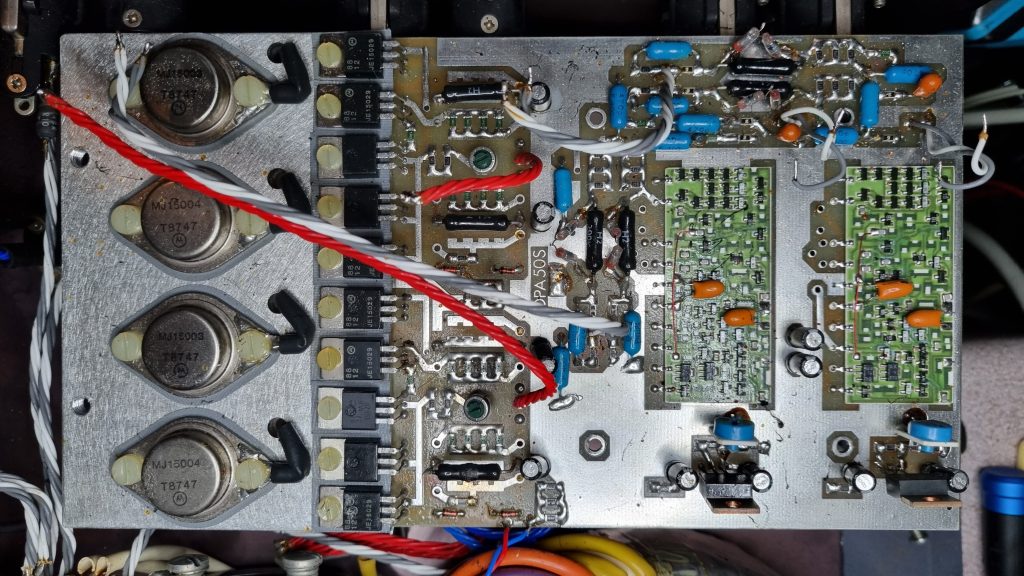
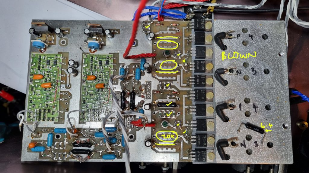
Let’s have a look inside. There’s a pair of complementary MJ15003/MJ15004 output transistors, and oops some burned out resistors in the middle. One of them got so hot it had clearly melted the solder it was ‘standing in’ and fell on its side!
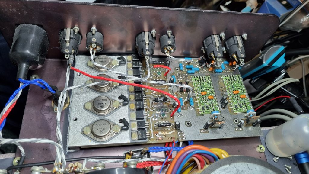
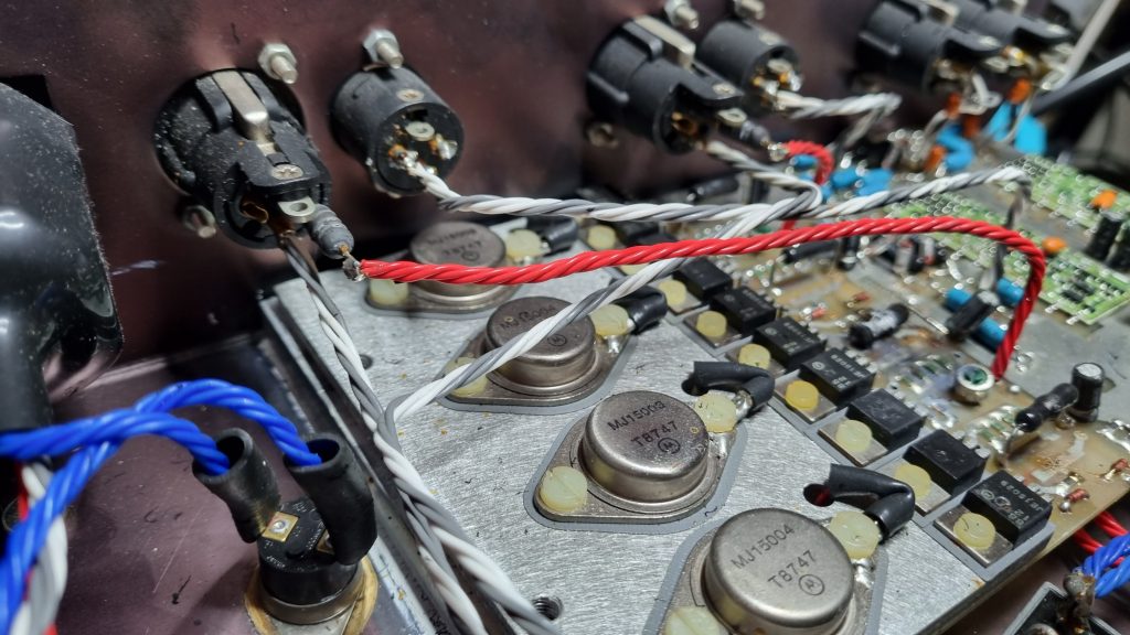
Closer up view of the output transistors, date code week 47 of 1987 🙂
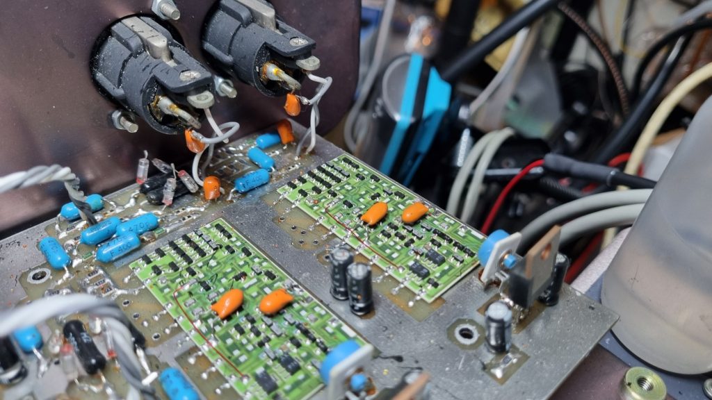
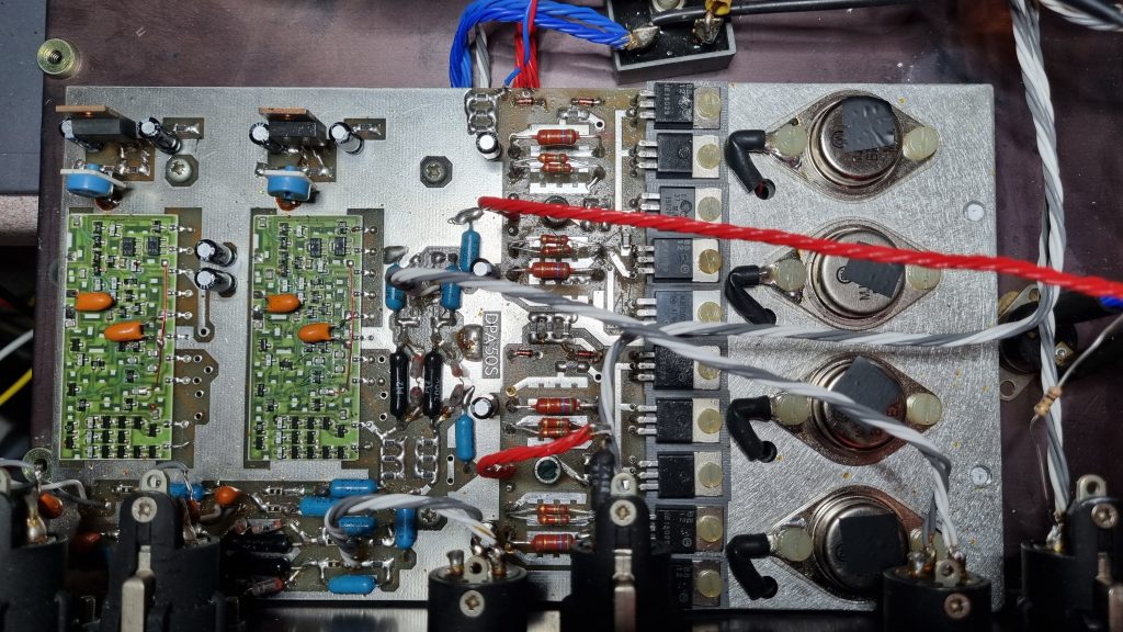
This preamp has some custom discrete op-amp input modules:
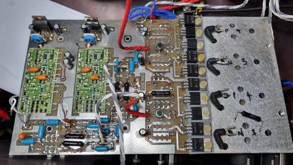
Got the board out and took out the fallen resistor to check over other things.
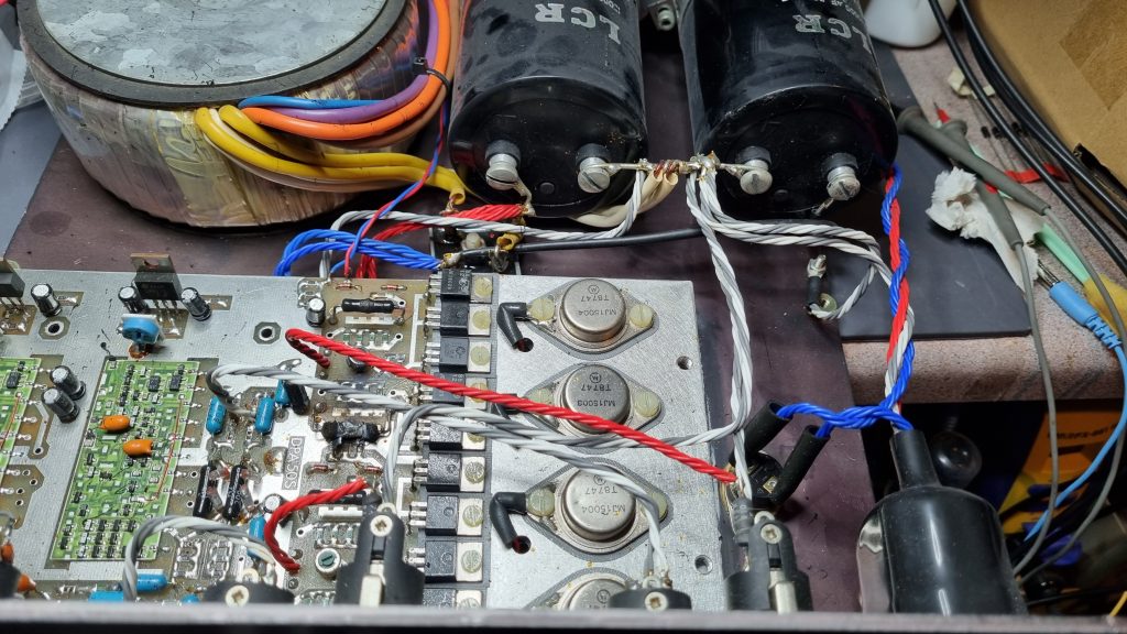
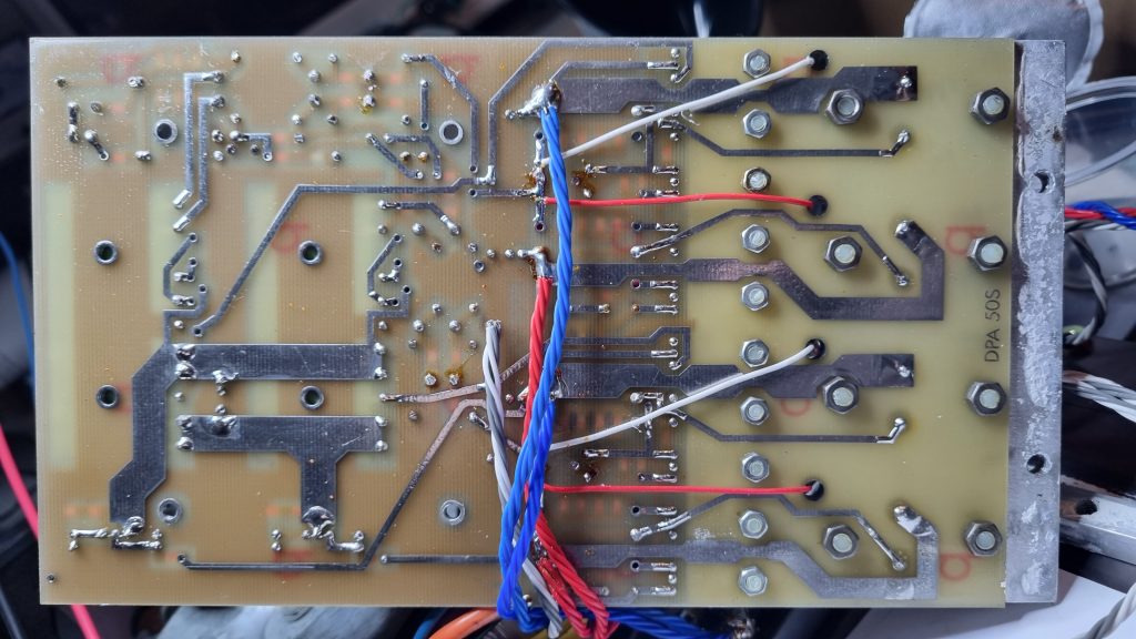
Reverse side of the board:
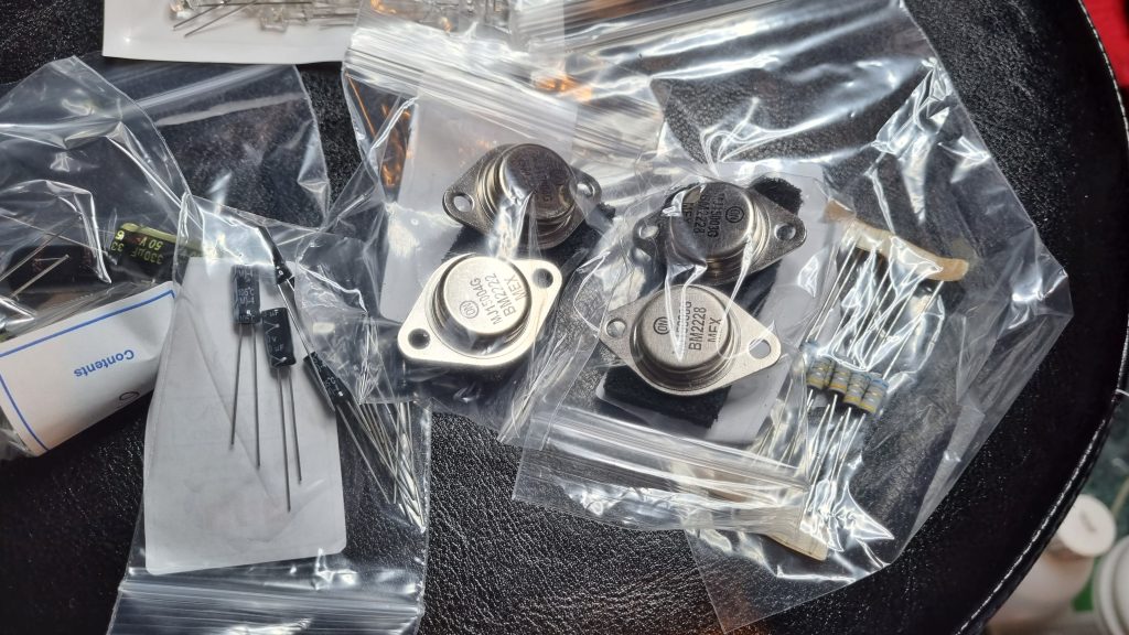
Unfortunately a pair of output transistors had gone short circuit too. Replacements at the time quite expensive but important not to get fakes, thankfully these were still available from local distributors CPC. Swapping all four makes sense (a bit like you wouldn’t change old springs on just one side of a car suspension).
6 ohm resistors of a suitable size were hard to find so got some 6.8R fusible resistors (later revised to 5.6R), and a few caps to replace the 10uF bypass ones that were reading out of spec:
Removal of faulty components…
I tried looking for service information for this unit as reverse engineering the amp wasn’t making a lot of sense (this amp also uses special feedback cables from the speakers). There were also parallel banks of 4 x 3R SMD resistors to make up the 0.75R emitter resistors, one lot of those were reading 20K across them. a 1R SMD resistor between T3-T4 on my scribbled diagram was open circuit on the main failed channel.
Below is what I’ve managed to scribble on tracing the output stage (may not be 100% complete)… Kinda makes a bit more sense from what I now understand on the current dumping style, seems to be a fixed bias current source set up by two diode voltage drops on T1 and 15R resistor, into T3 (+base of T2), with signal input on T5 – Driver/output T2 and T4 with main output transistors taking over for larger current flows through the increased voltage drop on the 6R resistors.
The parallel 3R SMD make up the 0.75R emitter resistors on T2 and T4 (these were both open on the failed channel, and high resistance on the NPN side T2 of the remaining channel)
Not sure what sort of alignment is needed on the 10R presets though (in-circuit those pots measure approx. 4.2R on failed and 3.6R on remaining channel) – is that more a 0V DC offset adjustment with the bias/idle current being fixed – feels a bit that way (but may have missed something)?
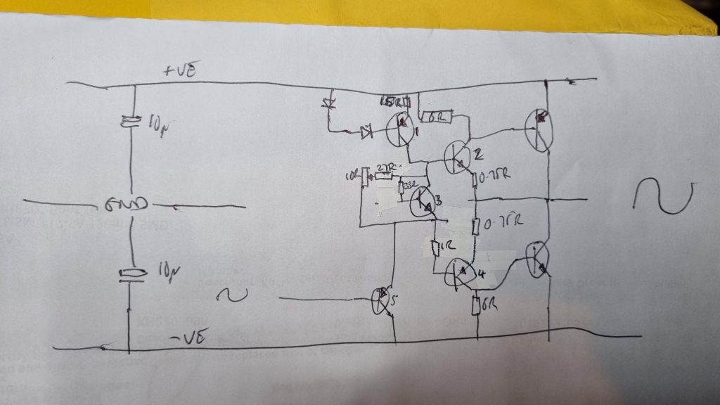
There is also 5R (3x15R SMD in parallel) from base to ground on T5 omitted in the above. T5 on one channel had also gone short C-E
I think may have found the failure mode, at least a contributory factor, when I was checking the 3R0 paralleled SMD resistors (the blown channel they were all open), I found one side on the good channel almost fully open circuit (20K vs 0.75R), with the 6R0 ‘air mounted’ resistor slightly high, suggesting overcurrent. I suspect it’s a runaway style failure as these increase in resistance (again not traced the circuit yet) until eventually they burn out and overdrive the output transistors to destruction.
I managed to get in touch with Martin Clark at Acoustica, who has a lot of experience with these amps. He didn’t recall seeing that internal layout before though! It is a very early example. He was very helpful in advising use of 5.6R resistors so these were ordered to use instead of the 6.8R ones, and advice on the speaker+feedback wiring required and some further info:
There are two preset pots on each channel: the one near each of the discrete opamp, sets DC offset at the output. This is, should hold, very very stable, and you can finesses that as much as you like on test.
Bias is set using the other pot. Aim for 350mV across either of the two 5R6 resistors fitted. Check/set other channel for same figure. Again, this should hold very closely over span of warm-up to hot on test, last time I opened mine up after 5yrs continuous use all were within 3mV. Given the way the output stage operates, and the galumphing amount of nested feedback wrapped-around – funnily -enough it is not that critical.
Initial testing after component replacement (decided to use pair of 1.5R in parallel rather than 4x3R SMD so a bit of a higher wattage rating) :
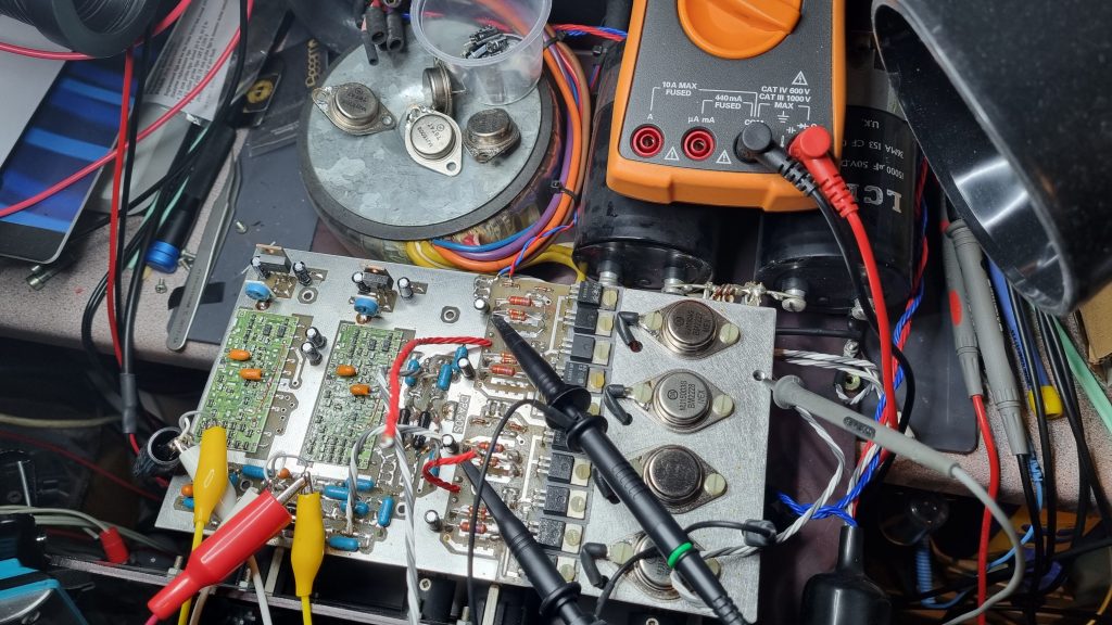
As for bias, after adjustment to 350mV with the lower 5.6R parts – power from cold goes from about 280mV, reaching about 420mV before settling back down to 350mV, on both channels… DC Offset is about 5mV on one and 60mV on the other. Adjusting the neg rail pot (assume it’s that, ones near the opamp boards) gets marginal, if any, adjustment. I’ve pretty much left them as they were (voltages on output approx. 36.9V and -36.8V)
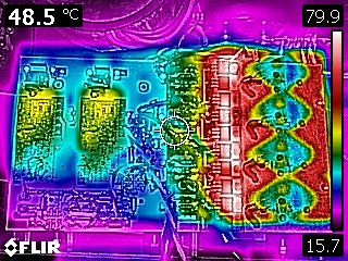
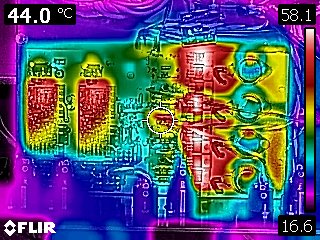
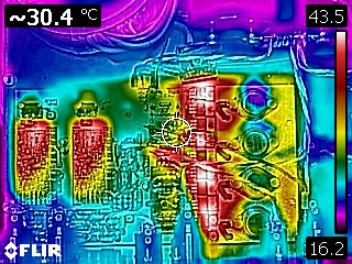
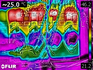
A bit of black tape attached to the output transistors for thermal imagery (for emissivity reasons – otherwise the shiny surface acts like a reflector instead)
Tempatures seem pretty even across both channels and nothing looking too horrendous
A 3W wirewound 0R1 resistor on the output sockets had also gone open, replaced with Tyco ER74R10KT to closely meet the original, and all tested ok.
Important to note that the speaker and feedback wiring NEEDS to be matched – if somehow the feedback plugs get crossed over between channels, this may cause a big DC offset to appear at the speaker outputs, word of warning!